
BYD Die and Mould in Beijing is BYD group’s internal competence center for stamping tools, producing high quality tools for BYD Motors and external OEM customers. BYD uses AutoForm’s simulation software for digital process engineering to virtually predict and solve issues before they occur on the shop floor.
Die spotting is one of the most critical and time-consuming elements in the manufacturing and verification of die stamping. The process engineer and tool designer define initial dimensions and tolerances according to the die surfaces to be retouched. Generally, the trial force applied during spotting is considerably lower than that of the production press, as the aim is not to obtain a part free of defects but to check the contact surfaces between the closing and bottom of the die. For this reason, it was surprising to see obvious waves and wrinkles in the binder area of a wheel house inner in the tool tryout shop (see Figure 1) — especially since the tool’s spotting status after binder closing was flawless , as shown in Figure 2. The first trials to solve these wrinkles by increasing the blank holder force failed . Mr. Hu Chungang from BYD Die and Mould and Mr. Gao Jiangtao from AutoForm China report how they succeeded in rescuing this wheel housing project.
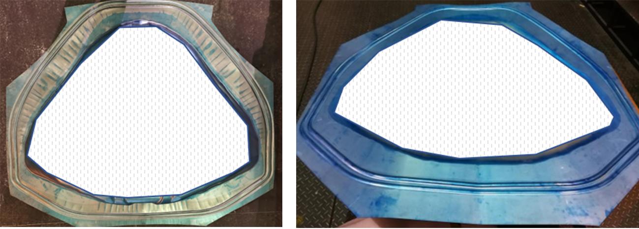
Figure 1. Binder status at bottom Figure 2. Spotting status of binder
Early in the simulation analysis, no obvious problems were found according to the Wrinkles, Surface Defect Height and Visual Check of the forming process. As shown in Figures 3 to 5, the Wrinkles values are essentially 0, the Surface Defect Height values less than 0.1 and the wrinkle risk area in the red circle does not match reality; no obvious waves are found in the forming process. If the evaluation is based on these results, there will likewise be no obvious wave in tryout. 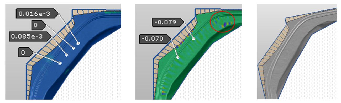
Figure 3. Wrinkles results Figure 4. Surface Defect Height results Figure 5. Visual Check
In the thinning distribution diagram shown in Figure 6, there is an obvious dividing line on the binder area. The thinning is different on either side of the dividing line, with the larger thinning caused by the material flowing through the drawbeads. This area also matches the wave area. The Minor Stress results then reflect uneven material flow, meaning this area has a large negative stress, as shown in Figure 7. Excessive local thinning causes a gap between the sheet metal and the die surface in this area, which in turn causes waves due to negative stress.
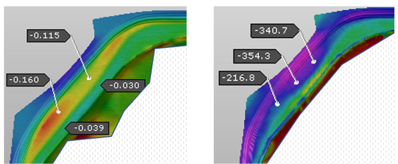
Figure 6. Thinning results Figure 7. Minor Stress results
The cross-section inspection in the wrinkled area (Figure 8) shows that the corresponding relationship between the thinned part and the die surface is wavy (the arrows point to gaps between the upper and lower surfaces of the part and the die). But with such small absolute heights, these waves can hardly be recognized as surface defects.
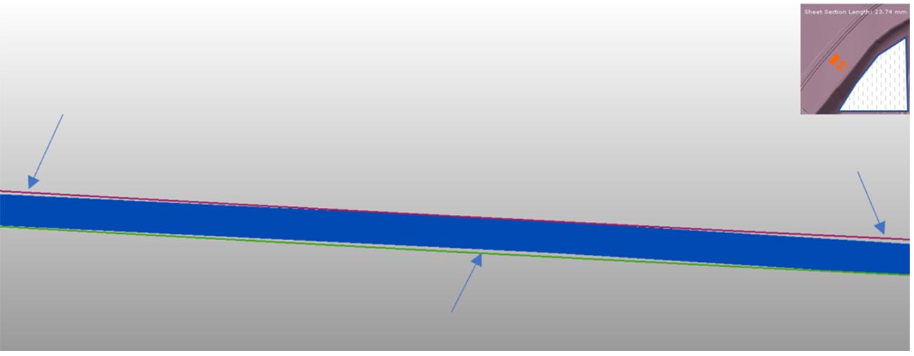
Figure 8. Cross-section in the wrinkled area
Based on those surface defect parameters, the simulation engineers began doubting the accuracy of the AutoForm simulation, as it wasn’t showing the same result as the first tryout (which is normal for first the first tryout). Importantly, the AutoForm results are based on a well-spotted die state with perfect press guidance and stopping accuracy, like a mass production press — which, of course, is not the initial case in the first tryout. Having the simulation, we can now try to match the simulated condition which will then produce the desired outcome.
Recalling that the aim of try-out is to begin to match the simulated conditions, the engineer used the contact distance from the AutoForm result parameters to check the contact state for die spotting. This perfect spotting state is generally required during the tool buy-off process, so process engineers usually report the contact distance based on well-spotted conditions for tryout engineers.
The contact distance reflects the distance between the upper and lower surfaces of the part and the die surface. When it is near or at the bottom, if the value of the contact distance in a certain area has obvious differences, it means that this area may be retouched for perfect spotting or the drawbead height adjusted for even thickness distribution. In this way, Mr. Hu and Mr. Gao could clearly map the spotting area based on the color. As shown in Figure 9, although the height of the waves is small, they are still obvious due to the many ups and downs.
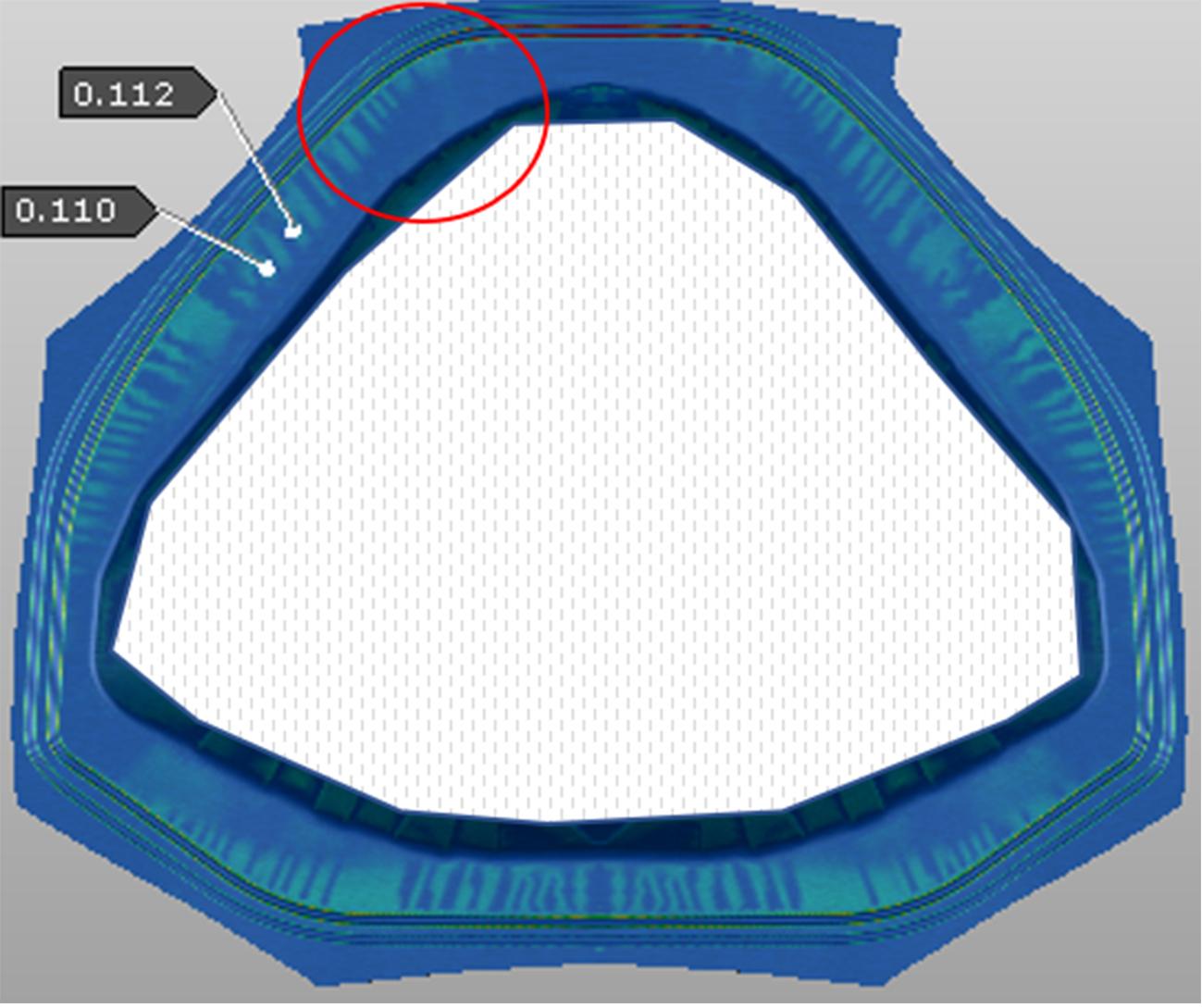
Figure 9. Contact Distance results
To resolve the wave issue during the on-site tryout process, first the binder area was reprocessed to address the thinning distribution. Next, the height of the drawbeads was reduced to then reduce the thinning of the binder area. The simulation and on-site results (Figure 10) show an obvious resolution of the problem.
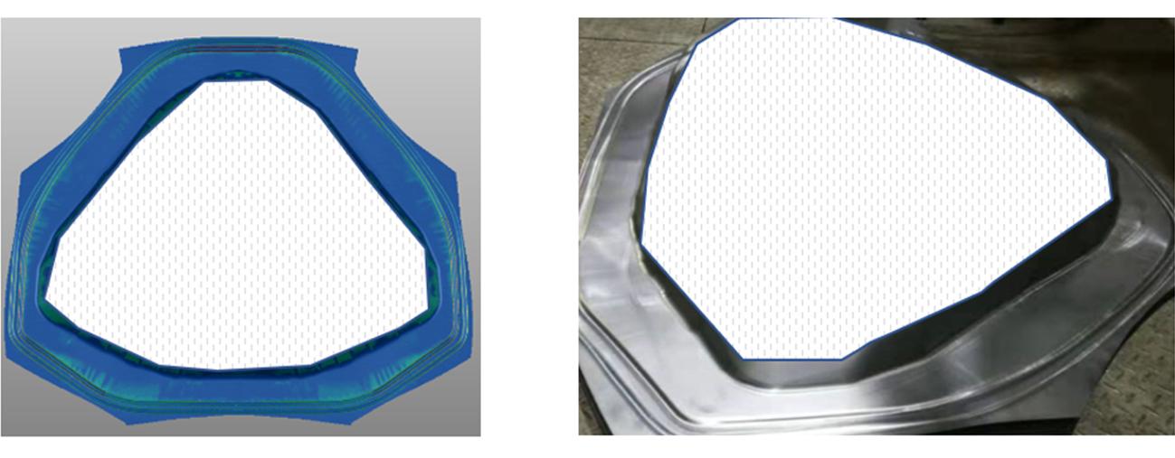
Figure 10. (Left) Contact Distance after reducing drawbeads (Right) Actual status after reducing drawbeads
Through this case, BYD Die and Mould realized that surface defect parameters they were using are not intended to check part quality under the binder area in the tryout phase. Instead, a contact distance map may be used for die spotting to guarantee a quality part free of surface defects in mass production. The AutoForm simulation always reflects production, while tryout is a process of fine tuning and getting to the simulated condition. BYD Die and Mould intends to add a contact distance map to the future standard process for die spotting in tryout.


?")


