
The Class A surface determines a consumer’s first impression of the quality of the entire product, so it should be perfect without any defects. But technically, it is very challenging to identify, quantify and find a solution to achieve the ideal quality.
In this article, we will be categorizing surface quality issues and explaining how to identify them using simulation technology, according to our experience on skin panels.
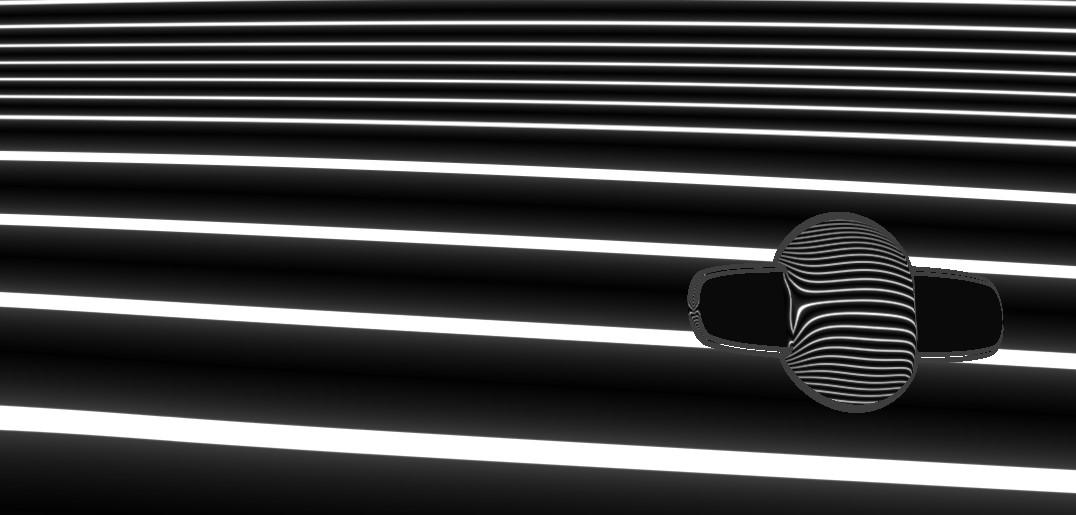
Fig. 1: Highlights (zebra lines) of a door outer panel represent the surface quality
1. Wrinkles
Sagging occurs during locating part, which causes unwanted bending and distortions during closing, forming permanent marks on the visible side of the panels. This wrinkling issue can be resolved with optimum binder surface and drawbead layouts.
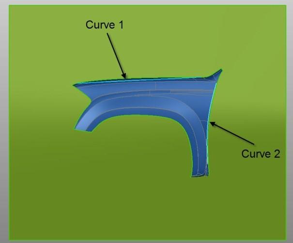
Fig. 2: Binder surface layout with part curvature
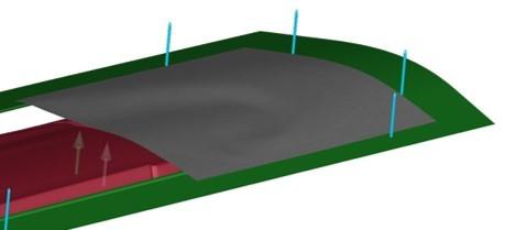
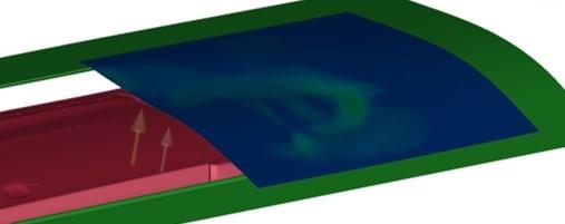
Fig. 3: Mechanism to cause permanent surface distortion with initial wrinkling
2. Sink marks
The skin panels have relatively large flat areas that are vulnerable to deformation from usage. In order to pass dent resistance and oil canning, the outer panel should be sufficiently stretched. For that reason, a minimum strain hardening requirement must be maintained for these kinds of panels, to increase the strength of the panel rather than increasing the thickness by adding weight or increasing the steel grade with low formability. A certain plastic strain is required for dent resistance and can be used for sink mark evaluation.
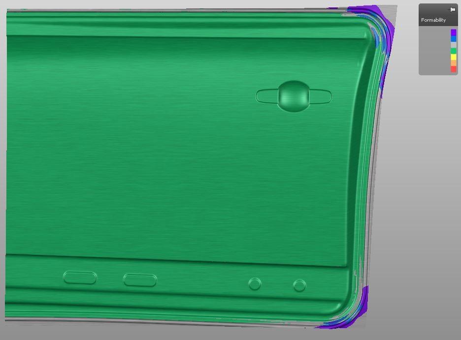
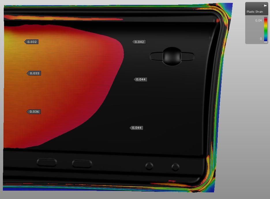
Fig. 4: Plastic deformation is required for dent resistance
3. Skidmarks
Depending on the material properties, a certain amount of pressure will start to deform the contact side of the metal, leaving permanent marks on the panel. If these marks are on visible zones, they will cause quality issues. They either need to be eliminated with a precise tribology strategy or by polishing after manufacturing; however, the latter requires a larger time and cost investment. It’s critical to check for tool skidmarks, especially on small radiuses, as these will create defects on the surface due to friction.
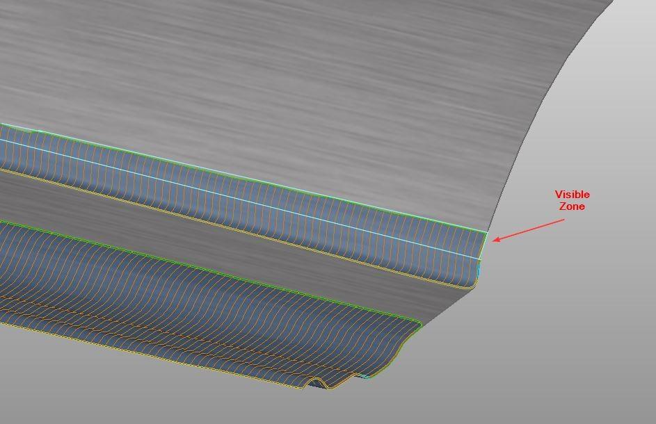
Fig. 5: Skidmark check
4. Feature slips (Double line: Shockline)
Initial local thinning happened at small character line radius slides nearby final formed character line radius. In this case, the formed shape will be forced into flattening again. But in accordance with the laws of physics, the deformation cannot be totally reversed. As a result, the sharp from cannot be achieved as desired from the CAD data, meaning the panel will deviate from its intended appearance. This will result in a quality issue after painting.
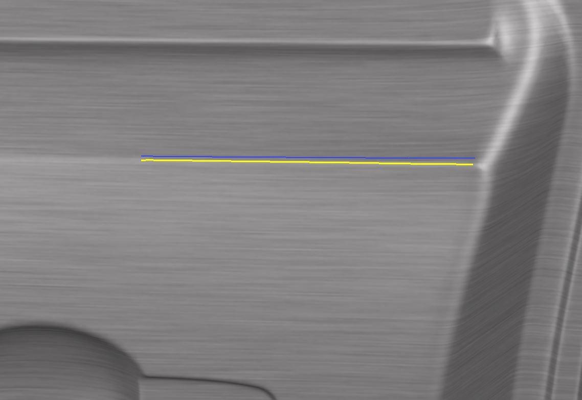
Fig. 6: Feature line slip check with local thinning
5. Surface distortion
Although a very small amount of springback (~0.1 mm) will not impact dimensional accuracy, it will still cause surface defects on nearly flat (small curvature) areas. These primarily occur as small dents on the surface, with circular, ellipsoid, or free shapes. And local elastic buckling from uneven directional material flows around embossing areas reflects low surface quality.
These defects are detected by rubbing flat, rectangular grindstones on the panel and observing the marks produced around non-contact areas. They are difficult to overcome, usually removed or reduced through more strain hardening, ironing, or local form changes.
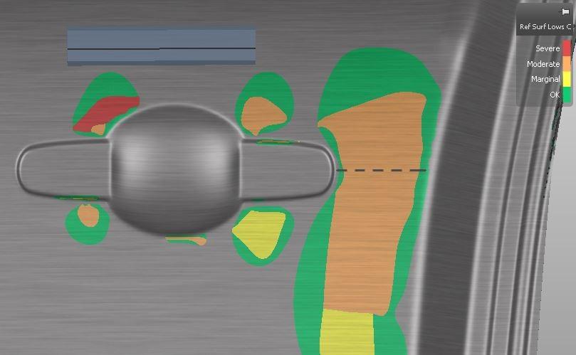
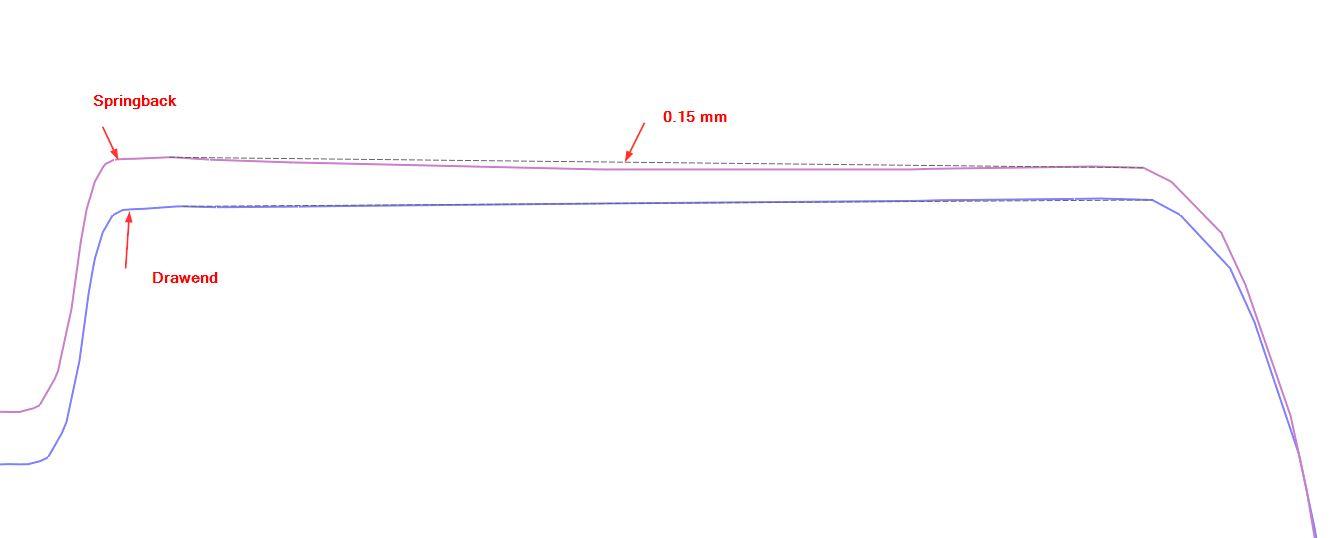
Fig. 7: Surface lows and stoning inspections
6. Flanging & forming wrinkles
The first drawing operation generally completes the forming of the panel. Except for trimming in operations, there is a certain amount of forming remaining for operations such as flanging and restriking. During these operations, the minimum contact areas are used for holding the panel so it does not experience further deformation. But even so, the forming operation itself makes some changes on stress fields, which may cause additional springback on the panel. These behaviors must be well observed and kept under control.
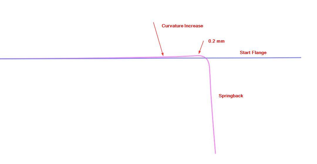
Fig. 8: Flanging after draw and trim operations may affect the shape on the main surfaces, especially if there isn’t enough stiffness on the part
These are all the major issues a stamping engineer may encounter during Class A panel process design. Each one must be handled separately, but the solution to one problem can make another problem worse. As a result, it is generally not easy to solve all the issues in their entirety but it is possible to optimize to an acceptable target level.


?")


